US6965157B1 - Semiconductor package with exposed die pad and body-locking leadframe - Google Patents
Polymers, Free Full-Text
Delamination in epoxy coated sterilized ACF interconnection after 85/85

Electronics, Free Full-Text

Figure 1 from Design Guidance for the Mechanical Reliability of Low-K Flip Chip BGA Package

Sn–Bi–Ag Solder Enriched with Ta2O5 Nanoparticles for Flexible Mini-LED Microelectronic Packaging

PDF) Evaluation of the Delamination in a Flip Chip Using Anisotropic Conductive Adhesive Films Under Moisture/Reflow Sensitivity Test
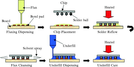
Flip Chip Underfill: Materials, Process, and Reliability

US8951840B2 - FCOC (Flip Chip On Chip) package and manufacturing method thereof - Google Patents

Micromachines, Free Full-Text

Printed circuit board embedded power semiconductors: A technology review - ScienceDirect

Polímeros: Ciência e Tecnologia (Polimeros)1st. issue, vol. 33, 2023 by Polímeros: Ciência e Tecnologia (Polimeros) - Issuu

Epoxy Potting Compound, 25 milliliters Dual Dispenser

Adhesion-Delamination Phenomena at The Surfaces and Interfaces in Microelectronics and MEMS Structures and Packaged Devices, PDF, Adhesion

Electronics, Free Full-Text