Figure 15 from The surface characteristics of under bump metallurgy (UBM) in electroless nickel immersion gold (ENIG) deposition

Building Solder Bumps on GaAs Flip Chip Schottky - CS Mantech
Practical Components

US7800240B2 - Under bump metallurgy structure and wafer structure using the same and method of manufacturing wafer structure - Google Patents

PDF) The surface characteristics of under bump metallurgy (UBM) in electroless nickel immersion gold (ENIG) deposition

Se-Young JANG, Vice Pesient, Ph.D, Samsung, Seoul

Se-Young JANG, Vice Pesient, Ph.D, Samsung, Seoul
Micromachines, Free Full-Text

Kyung-Wook PAIK Korea Advanced Institute of Science and

US20030067073A1 - Under bump metallization pad and solder bump connections - Google Patents

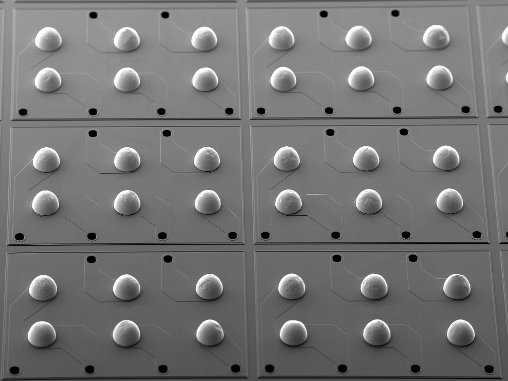
Figure 1 from Plasma reflow bumping of Sn-3.5 Ag solder for flux-free flip chip package application

Kyung-Wook PAIK Korea Advanced Institute of Science and

The surface characteristics of under bump metallurgy (UBM) in electroless nickel immersion gold (ENIG) deposition - ScienceDirect

PDF) The surface characteristics of under bump metallurgy (UBM) in electroless nickel immersion gold (ENIG) deposition
Solder Balling for WLCSP and Flip Chip Interconnects