Do you know what PCB via size you should use in your PCB layout? We’ll look at a few simple ways to answer this question.

US9465412B2 - Input device layers and nesting - Google Patents
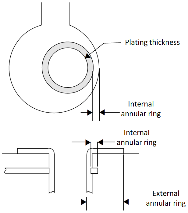
PCB Via Size and Pad Size Guidelines, Zach Peterson, Blog
OPENING SESSION - ismrm

When to Use Via in Pad

Altium Designer Set Default Via Size - Design Talk
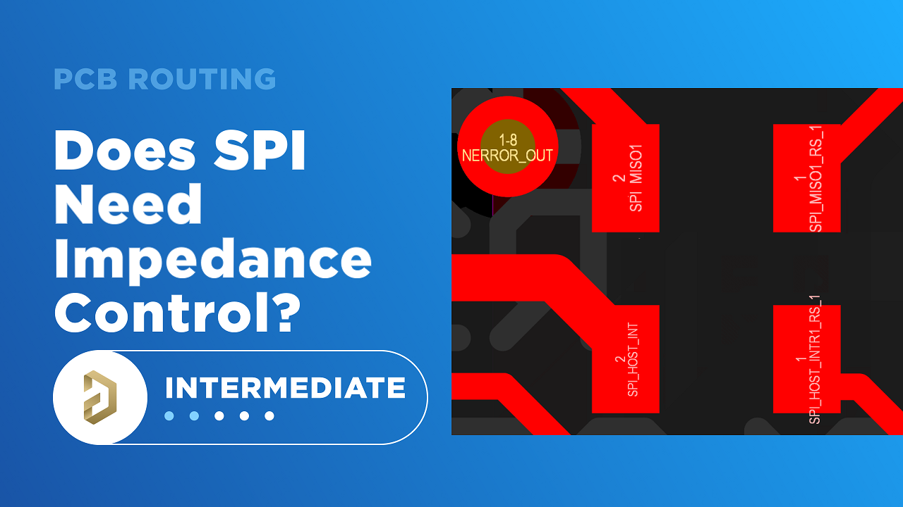
Is There an SPI Trace Impedance Requirement?, Zach Peterson

The Universal Sea - The Art and Innovation Guide Against The Plastic Epidemic by The Universal Sea - Issuu

ESR_Calculators__th.jpg
PCB Via Size and Pad Size Guidelines, Zach Peterson, Blog

Tools Source Book Volume 1 by Federal Buyers Guide, inc. - Issuu

Journal of Surface Mount Technology - SMTA

Review request - ESP32 WROOM module based RS232 controller : r/PrintedCircuitBoard
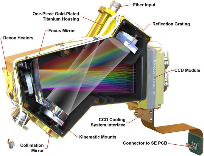
The SuperCam Instrument Suite on the NASA Mars 2020 Rover: Body Unit and Combined System Tests

Design007 Magazine :: I-Connect007