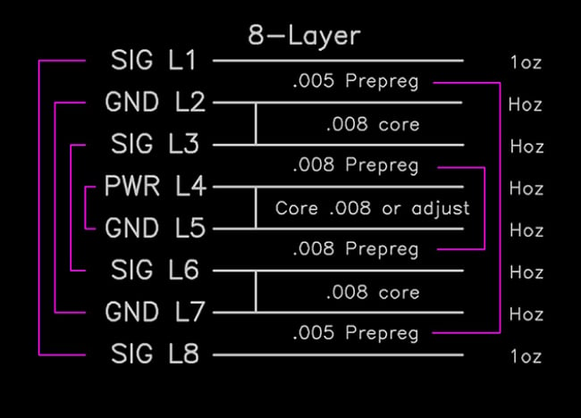
Balancing layers in your PCB layout stack-up, which both layer surfaces and cross-sectional structure of the circuit board are reasonably symmetrical.
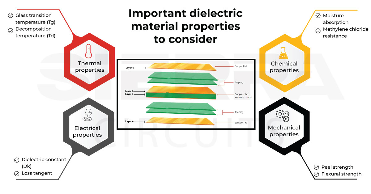
PCB Substrates: Knowing PCB Dielectric Materials

EasyEDA Std Tutorial
How to Determine the Number of Layers in PCBs
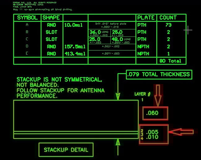
Balancing Layers in Your PCB Layout

Two Layer PCB Design: Tips and Best Practices – Hillman Curtis: Printed Circuit Board Manufacturing & SMT Assembly Manufacturer
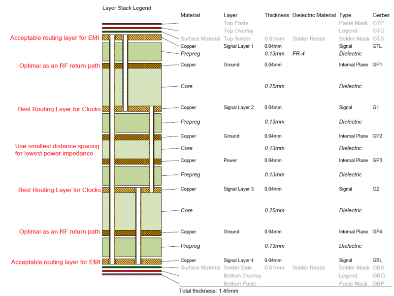
PCB Stacking Techniques: Determine PCB Layers and Design an

What are printed circuit boards made of?
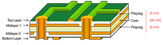
How to Design and Fabricate the Best 4 Layer PCB Stackup with
The Mysterious 50 Ohm Impedance: Where It Came From and Why We Use

Cash Coupons & Balance - How do I use PCBWay Cash Coupons/Balance
Epec's Blog Printed Circuit Boards (7)

Gigabit Ethernet 101: Basics to Implementation, Blogs